Driving a VFD with the HV5812
<-- Fiat Lux! | Shady Characters -->
Having actually lit up the VFD on the breadboard, it’s time to actually drive it with the HV5812 driver chip I’m planning to use in the finished clock.
First I wired it all up:
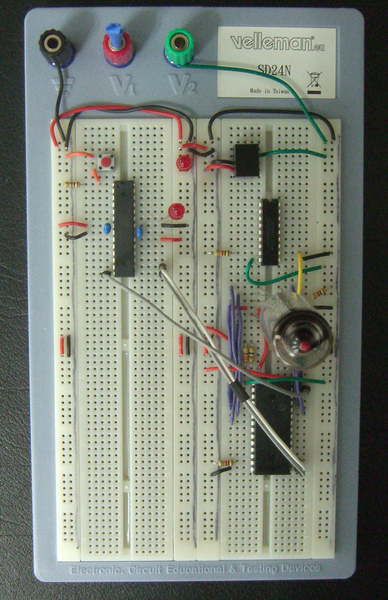
In the left column:
- Reset button and pullup resistor for the ATmega328
- ATmega328 microcontroller. The brains of this operation.
In the right column:
- 5V DC voltage regulator
- High voltage driver for the VFD grids, currently pulled up. Eventually I’ll control this with the MCU so I can multiplex the VFDs in a 2x2 configuration.
- The VFD and the resistors that provide 1.5 V across the filament from the 5V bus.
- The HV5812 driver.
If I were setting this up again, I’d put the 12V bus on the left side of the breadboard instead of the right since both the HV5812 and the high voltage driver take high voltage in on the left side. Whoops.
The wires are color coded as follows:
- Red: +5VDC
- Green: +12VDC
- Black: ground
- Orange: reset for the MCU
- Purple: VFD anodes
- Yellow: VFD grid
- Gray/White: logic level between the MCU and the HV5812.
The HV5812 is pretty straightforward. It’s a 20 bit serial input shift register, with each bit corresponding to one output pin. If you want to daisy chain two of them together, there’s a DATA_OUT pin that you can connect to the DATA_IN pin of a subsequent HV5812.
Data gets shifted in on the rising edge of the clock, and a rising edge on the STROBE pin latches the current state of the shift register on the output pins. There’s also a pin to blank the outputs without affecting the state of the shift register or outputs. I’ve pulled it down with the resistor in the lower left corner of the chip.
As noted earlier, the through-hole version of the HV5812 is .6” wide. It really is prety large. I’m doing all of the prototyping with the through-hole version, but when I go to layout the PCBs, I may switch to the SOIC version if it results in a nicer overall package.
I’m using the GPIO pins on the MCU and toggling them as needed to drive the HV5812 for now. The ATmega328 is running at 8MHz divided down to 1MHz, and the HV5812 will take data at 5MHz. To allow the required setup time for DATA_IN, I’m setting or clearing its output in one line, and then setting the clock in the next. If this compiles down to two OUT instructions (as is the case when there’s already a register containing the value I’m outputing), I’m sending data at 500KHz.
The quick and dirty code to validate all of this is here
Next time: letters and numbers!